Momentum: GNSS, 9-DOF IMU, Barometer Sensor Shield
This document also applies to Momentum Lite which the same board design, with reduced components (no GNSS).
Table of Contents
1 Overview
1.1 Bill of Materials (BOM)
| Manufacturer Part Number | Manufacturer | Description | Quantity | Notes |
|---|---|---|---|---|
| STM32L432KC | STMicroelectronics | 32-bit MCU | 1 | |
| CP2102N-A02-GQFN24R | Silicon Labs | USB 2.0 to UART Interface | 1 | |
| BNO086 | CEVA Technologies, Inc. | 9-DOF IMU | 1 | |
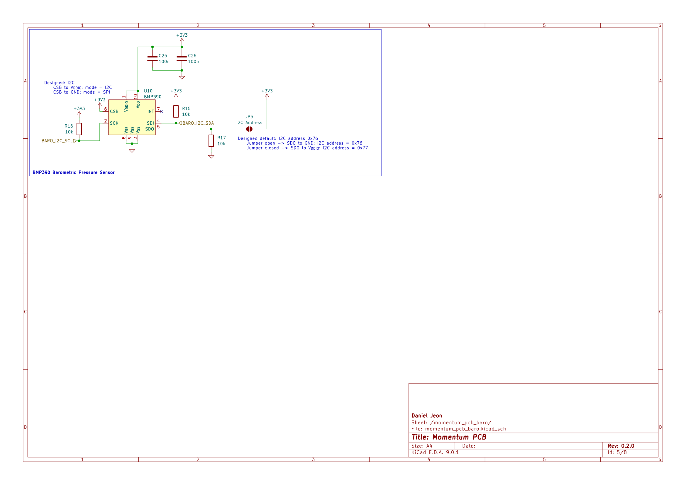
| BMP390 | Bosch Sensortec | Barometric Pressure Sensor | 1 | |
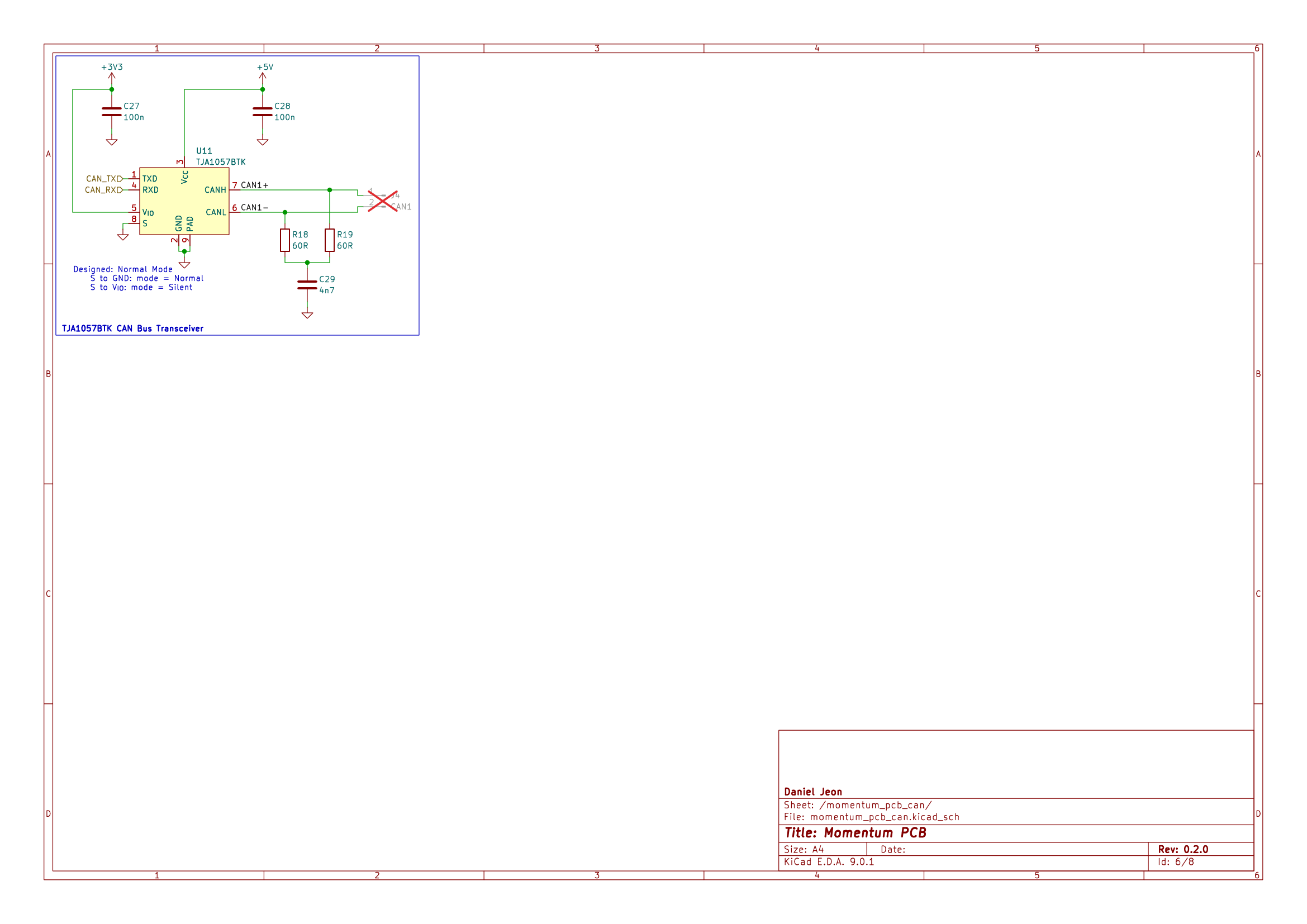
| TJA1057BTK | NXP USA Inc. | CAN Bus Transceiver | 1 | |
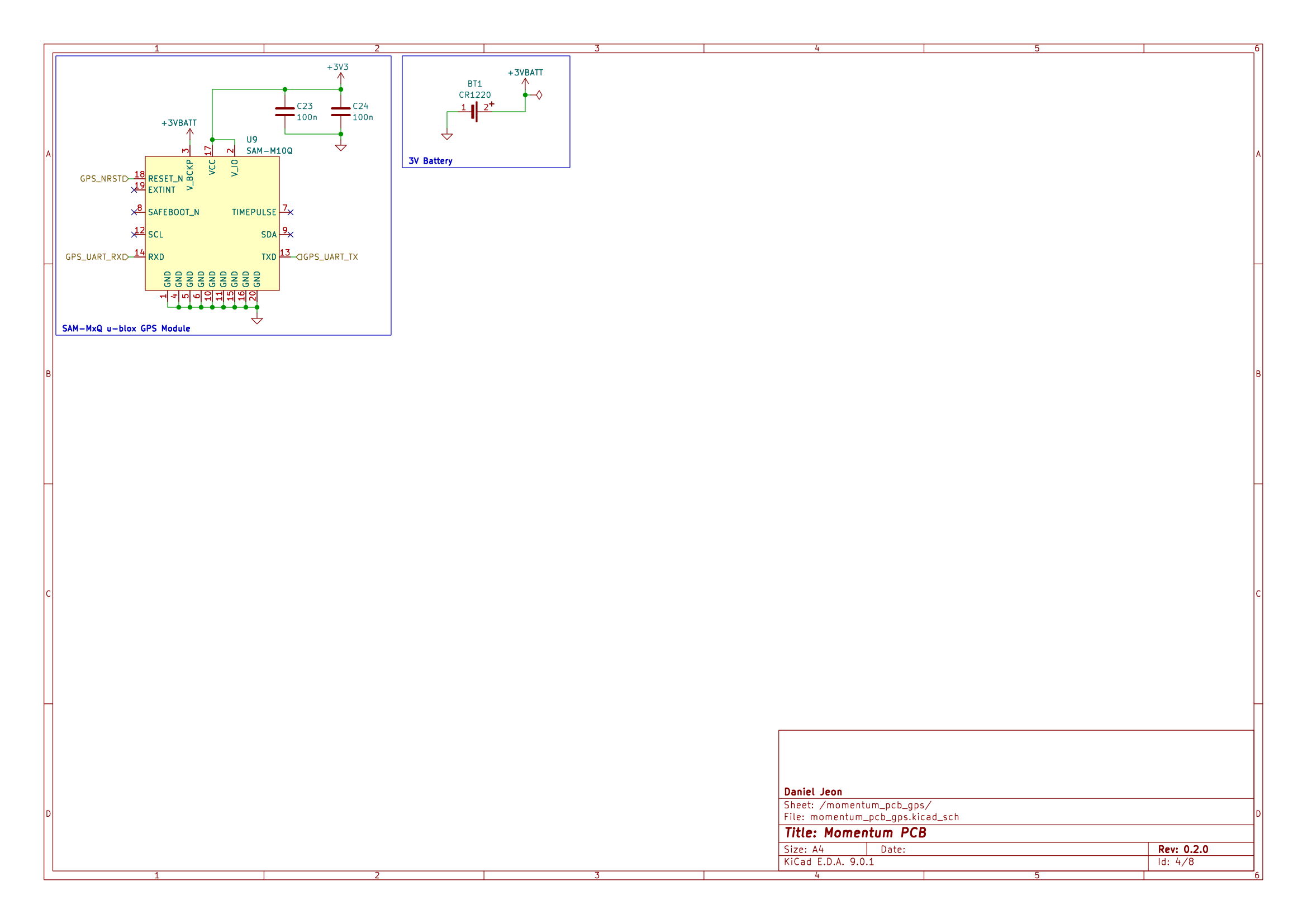
| SAM-M10Q | u-blox | RF Receiver Galileo, GLONASS, GPS | 1 | |
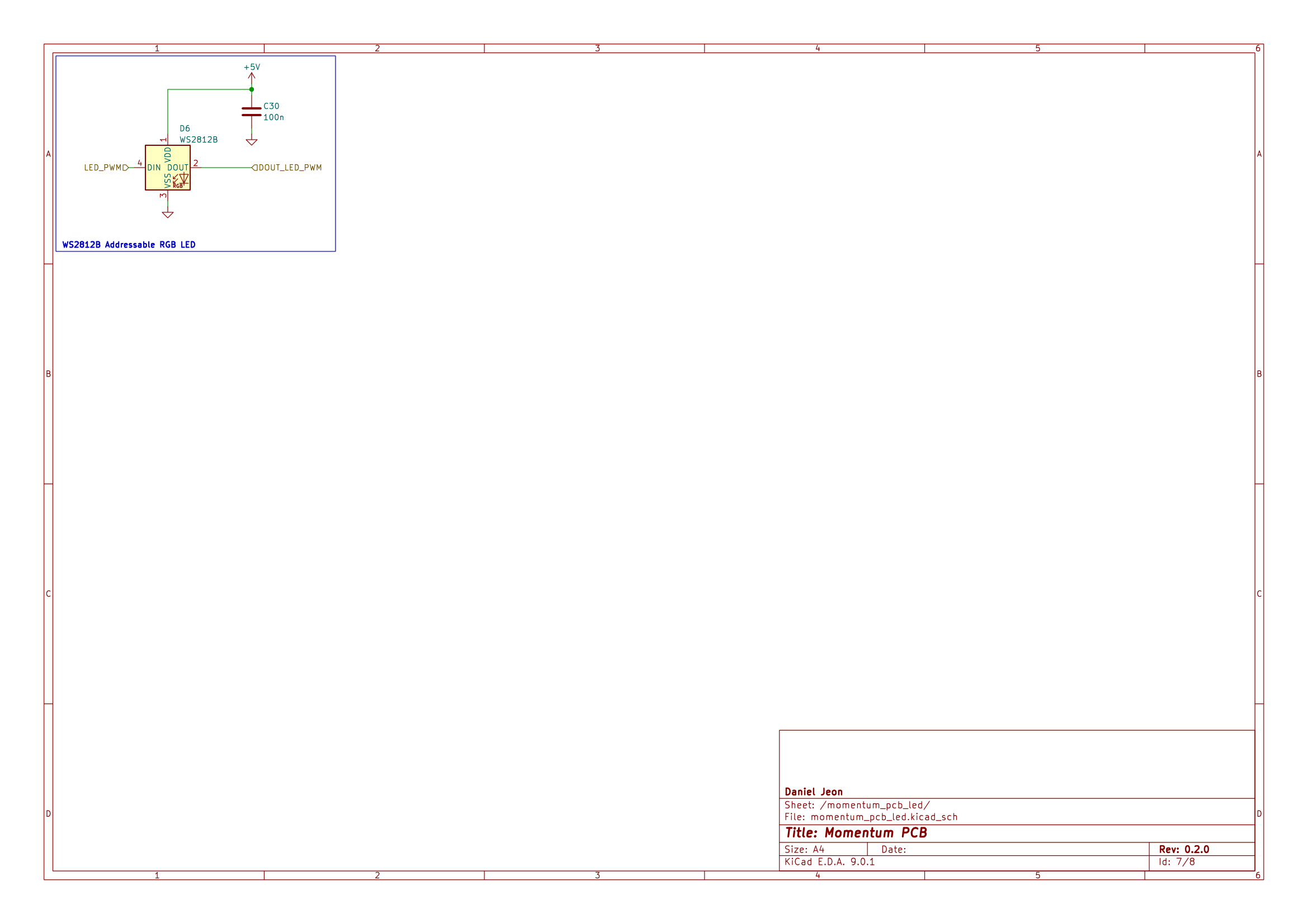
| WS2812B | (Various) | PWM Addressable RGB LED | 1 |
Note: Momentum was originally designed for the BNO085, however hardware files were updated to reflect use of the newer BNO086. Firmware is cross compatible for both the BNO085/6, however source files maintain the use of the "BNO085" naming.
1.2 Block Diagram
2 Board Specifications
2.1 Connectors
Connectors fixed by hardware (PCB traces or the connector itself).
| Connector | Ref | Description |
|---|---|---|
Tag-Connect TC2050 |
J1 | SWD programming/debug connector |
BOOT0 jumper |
J2 | Open for run flash memory (pull-down on open) |
USB-C |
J3 | USB-to-serial programming/debug, secondary 5 V source |
CAN1 |
J4 | Pin 1: CAN1 High, Pin 2: CAN1 Low |
2.2 Switches & Jumpers
User controllable hardware and/or firmware driven inputs.
| Switch/Jumper | Ref | Description |
|---|---|---|
Sensor Hub MCU reset button |
SW1 | Generic 6 mm TH button, push to reset |
5 V bypass |
JP1 | Closed = Short protection (schottky) diode pads, open = enforce schottky diode |
Level shifter V IO |
JP2 | 1 + 2 closed = 5 V, 2 + 3 closed = 3.3 V |
BOOT0 DTR bridge |
JP3 | Closed = CP2102N DTR BOOT0 control, open = Manual BOOT0 |
BNO086 clock select |
JP4 | Open = crystal, closed = external/internal |
BMP390 I2C address |
JP5 | Open = 0x76, closed = 0x77 |
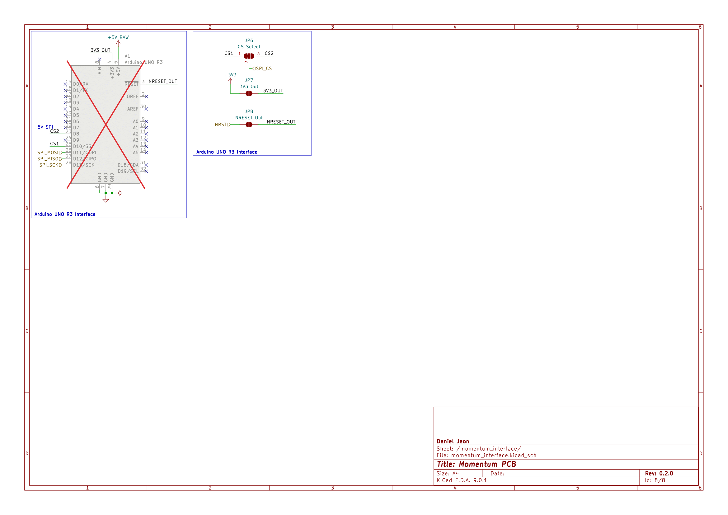
Interface SPI CS pin select |
JP6 | 1 + 2 closed = CS1 (D10), 2 + 3 closed = CS2 (D8) |
Interface 3.3 V output |
JP7 | Open = no output, closed = 3.3 V LDO output bridged |
Interface NRESET output |
JP8 | Open = no output, closed = STM32 NRST bridged |
2.3 Batteries
Onboard battery supplies.
| Battery | Ref | Description |
|---|---|---|
CR1220 battery cell |
BT1 | u-blox GNSS RTC and ephemeris RAM |
2.4 LEDs
LEDs used to show board status and/or user controllable.
| Test Point | Mark | Description |
|---|---|---|
UART TX |
Silkscreen: "TX" | Green LED: blinking = transmitting data |
UART RX |
Silkscreen: "RX" | Amber LED: blinking = receiving data |
5 V Supply |
Silkscreen: Lighting bolt | Amber LED: on = 5V pin, off = (only) USB-C |
WS2812B LED |
None | RGB addressable LED |
2.5 Test Pads
| Test Point | Ref | Description |
|---|---|---|
GNSS NRST |
TP1 | u-blox GNSS NRST net |
GNSS RX |
TP2 | u-blox GNSS RX net |
GNSS TX |
TP3 | u-blox GNSS TX net |
WS2812B LED PWM |
TP4 | DOUT from onboard WS2812B |
2.6 Power Supply
The board can be powered by either of the following methods:
- 5V pin via the Uno-style interface.
- Onboard USB-C connector.
2.6.1 5 V Power OR Switch
The 5 V supply is controlled by an OR-ing power switch (TPS2116DRL).
- The Uno-style 5V pin has priority: if ~1 V or higher is present, it is used as the source.
- If this condition is not met, the board automatically switches to the USB-C 5 V supply.
2.6.2 Optional 5 V Pin Supply Protection
The 5V pin supply can be optionally protected with diodes (not installed by
default). To enable protection, follow these steps:
- Cut the
5 V bypassjumper to remove the short across the schottky diode pads, ensuring use of the schottky diode. - Schottky diode required (designator
D1, footprint SMA).- Intended to provide reverse polarity protection.
- TVS diode required (designator
D2, footprint SMB).- Intended to provide short transient over-voltage clamping.
2.6.3 3.3 V LDO Supply
The 3.3 V supply is managed onboard by a dedicated 5 V to 3.3 V LDO, independent of any connected board.
If the user wishes to use the Momentum dev board's 3.3 V supply as an output
supply for low current applications, the Interface 3.3 V output jumper can be
bridged, allowing for 3.3 V to be supplied from the onboard LDO.
Warning: This modification should be evaluated for each specific application. Many development boards provide their own regulated 3.3 V output on the Uno-style
3.3Vpin. Connecting this pin in parallel with another 3.3 V supply can cause contention between the two outputs, potentially resulting in damage or unstable operation.
2.7 SPI Interface
All SPI pins interfacing with external boards are level-shifted. By default, the
SPI bus is shifted to 5 V. However, it can also be shifted to 3.3 V via the
Level shifter V IO 3-pad jumper.
See section 2.8 Level Shifter for details.
The SPI CS pin can be reassigned between Uno-style pins D10 (default) and D8
via the Interface SPI CS pin select jumper, allowing flexibility in resolving
pin conflicts.
2.8 Level Shifter
Note the level shifter interfaces with the SPI singals (CIPO, COPI, SCK and CS)
as well as the WS2812B PWM data line. Adjusting the Level shifter V IO 3-pad
jumper selects between 3.3 V and 5 V.
When set to 3.3 V, note that the WS2812B LED may become unstable. According to the WS2812B datasheet:
- DIN high >= 0.7 * VDD
- DIN low <= 0.3 * VDD
A 3.3 V logic-high signal may not satisfy the DIN high threshold, potentially causing reduced or unreliable functionality in this configuration.
2.9 STM32L432KC Flashing
The official STM32L432KC Momentum firmware is managed
here: momentum.
The STM32L432KC can be flashed in 3 different ways:
- SWD via Tag-Connect TC2050 interface.
- Hands-free UART bootloader via USB-C (CP2102N USB-to-UART).
- Manual BOOT0 jumper with UART bootloader via USB-C (CP2102N USB-to-UART).
For use of the USB-C UART bootloader interface, the custom flashing
software pyblasher is highly
recommended.
All three options are available by default, however it is suggested to use options 1 and 2 based on user preference.
Option 3 is applicable for users who wish to use the USB-C for as both a
serial and UART bootloader interface. In this method, the through-hole
BOOT0 jumper must be manually bridged to assert BOOT0.
See section 2.10 USB-C Serial Interface for details.
2.10 USB-C Serial Interface
The USB-C interface connected via the CP2102N USB-to-UART is primarily designed as a UART bootloader flashing interface, however it can also be used as a serial interface for simple communication to a desktop computer.
Due to the design for hands-free flashing, the STM32's BOOT0 is controlled by
the CP2102N's DTR pin. Consequently, when a serial port is established BOOT0
will be raised high, entering the bootloader. To prevent this behaviour, the
BOOT0 DTR bridge jumper must be cut, allowing for USB-C serial communication
without triggering the bootloader.
If the user wishes to still use the UART bootloader with this modification, the
BOOT0 must be asserted manually to enter the bootloader via the 2-pin
through-hole BOOT0 jumper.
3 Schematics
Download PDF: momentum_pcb-schematic.pdf.
4 CAD 3D Model
Download STEP: momentum_pcb-3D.step.